Dumping ROMs with Linux Boards
Non-volatile memory is used to store data persistently and this data may be either writable or read-only (ROM). ROMs are used in everything from video game cartridges to store executable game code, to firmware for your home printer. This type of data is typically inaccessible to a user as it's modification could permanently damage a product. Likewise, ROMs may also contain proprietary data that the manufacturer does not wish to distribute. If you're looking to reverse engineer software on a physical device, dumping the memory from ROM for analysis is extremely valuable. The integrated circuits (IC) for these memory modules come in different physical packages, but they all have some sort of pins including ground, power, and data. Additionally these ICs have a common communication protocol such as SPI, I2C, or Microwire. The premise of dumping ROMs is to access the pins of the memory IC, then communicate with it through its protocol to dump the data. There are different approaches to this, however they all fundamentally do the same thing.
Memory IC programmers are quite common to use for data extraction, since they are likely the tool used to flash them in the first place. Such programmers like the DataMan and XGecu are popular choices, but they can be quite expensive and software is closed source. Cheaper options also exist such as the CH341A, however you need to install closed source drivers - and the device itself is not robust. The approach presented in this article uses Linux on a single-board computer (such as Raspberry Pi) to connect the pins on the memory IC to a GPIO header. The GPIO header on these boards typically support both I2C and SPI which represent an overwhelming amount of memory ICs which use these protocols.
Irrespective of approach, the objective of using either a programmer device or a Raspberry Pi is to interface with the memory IC pins for communication. For instance if the memory IC is socketed onto the board (e.g. DIP), you can simply plug it into a programmer's ZIF (zero-insertion force) socket. If we're using a Raspberry Pi, we can rehost the DIP package in a breadboard and then wire the breadboard to the GPIO header. The same strategy applies for surface-mounted memory ICs without exposed leads (e.g. BGA); except there's an added step of desoldering and remounting in an adapter. Surface mounted chips with exposed leads (e.g. SOIC) may also be desoldered and re-hosted, however a clever approach is to attach a test clip. By attaching an IC test clip, each pin breaks out into a wire which can be routed to either a Raspberry Pi directly - or to a host adapter (e.g. a DIP board).
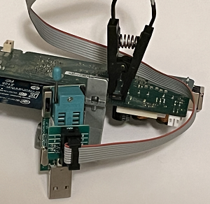
Above is an image of an attached IC test clip, connected to a DIP adapter board, socketed into a CH341A programmer
Identifying the Target
The memory IC will typically have a number in the package type denoting pin count. For instance a BGA-54 contains 54 ball pins, and a SOIC-16 chip contains 16 pins. For
non-volatile memory used as ROM chips, the three most prevelant types include flash (NOR and NAND), EEPROM, and EPROM. Flash memory is widely used as a ROM chip in SOIC-8 and SOIC-16 packages.
EEPROMs have been largely replaced by flash and may also be found as SOIC-28. EPROMs are now quite rare as they were replaced by EEPROMs; if they are soldered it's likely SOIC-8. EPROMs pre-date
the prevalence surface mount technology and is more commonly found as a DIP package. Unlike EPROMs, flash is found almost exclusively as a surface mounted device, although they are also
available in DIP packages. Below are two images of SOIC chips from common consumer electronic devices which I've extracted firmware from. On the left is a SOIC-16 flash chip from a home router,
and on the right is a SOIC-8 flash chip from my HP Envy printer.
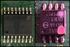
In addition to the package type, the memory IC will have nomenclature printed on the package itself. The nomenclature is not standardized, however generally speaking there are two sets of numbers
denoting size and communication protocol. The size denomination is in bits and not bytes, however the unit is unspecified - for instance 128 may mean 128Mb or 128Kb. The communication
protocol is synonymous with the series marking, and is typically the first identifier in the marking. Optionally a vendor id code will come before the series marking but they are the same part, e.g.
25Q128FVFG is the same as W25Q128FVFG ("W" vendor id is Winbond). Below is a table I derived from various sources and looking through memory ICs on
Mouser.
| Series | Protocol | Type |
|---|---|---|
| 24 | I2C | EEPROM |
| 25 | SPI | Flash, EEPROM |
| 27 | Parallel | EPROM |
| 28 | Parallel | EEPROM |
| 34 | I2C | EEPROM |
| 45 | SPI | Flash |
| 93 | Microwire | EEPROM |
| 95 | SPI | EEPROM |
Connecting the GPIO
When using a programmer, typically the memory IC is mounted in a socket directly or by using a conversion adapter. Connecting a memory IC to a GPIO requires mapping the pins appropriately. The table below maps a 25-series flash SOIC-8 and SOIC-16 chip against a J8 header, like you would find on a Raspberry Pi. As you may notice, only 8 of the 16 pins are used on the SOP16 mapping, and that's because RESET was omitted - whereas on SOP8 it shares a pin with HOLD. You may connect the RESET pin, however this allows you to translate SOP16 to SOP8 which is useful with programmers like the CH341A which only accepts DIP8. With this in mind, there are a couple popular DIP8 boards that are marked as being SOP16/8.
| SOP Name/GPIO Name | SOP8 Pin | SOP16 Pin | J8 GPIO Pin |
|---|---|---|---|
| CS/CE0 | 1 | 7 | 24 |
| DO/MISO | 2 | 8 | 21 |
| WP/VCC | 3 | 9 | 1 (3.3V) |
| GND | 4 | 10 | 9 |
| DI/MOSI | 5 | 15 | 19 |
| CLK/SCLK | 6 | 16 | 23 |
| HOLD/VCC | 7 | 1 | 1 |
| VCC | 8 | 2 | 1 |
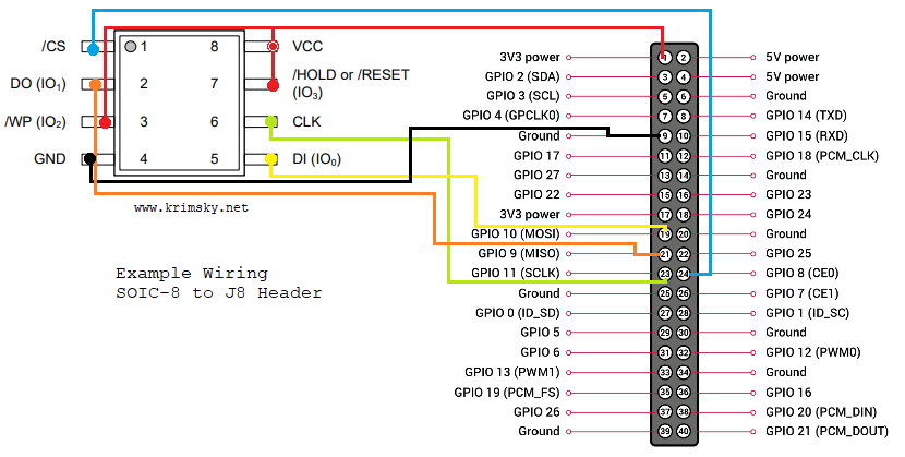
Sometimes having the visual also helps, so below is a wiring diagram going from the SOIC-8 memory IC to a J8 header. The 3.3V power pin was selected as an example, refer to the memory IC datasheet for the correct voltage. The voltages are usually within a broad range, but generally speaking ICs are 5V, 3.3V, 2.5V, and 1.8V. Some pins are also duplicated such as ground - in which case the specific pin doesn't matter. All the pins are 1:1 including DI (data in) on the IC to MOSI (slave input) on the J8, and DO (data out) to MISO (slave output). Setting WP (Write Protect) to VCC will enable it, you will not want to accidentally write to your chips. HOLD is active low which will essentially disable communication, so this needs to also be connected to power.
In-System Programming (ISP)
This section briefly goes over strategies for in-system programming, i.e. using a test clip. You have a choice as to whether or not you will supply power to the memory IC when the board is powered off, or to not supply power when the board is powered on. The power pin on the memory IC is connected to a rail, and more than likely there are other components that also use that rail. If you provide power to the memory IC, you may also be powering other ICs. In this scenario you may not have enough power to read the chip if you are providing power from a single-board computer, which is itself running off of USB power. Another potential problem is not getting a clean read because you're powering various ICs into an unknown state. I've found that when using a programmer like a CH341A, stepping-down the power (still within operating range) can improve read results; for instance reading a 3.3V IC at 2.5V. After trying different approaches, my preference is to not provide power and let the board power naturally - simply don't connect the vdd pin from the test clip. Additionally you can check if both WP and HOLD are high using a multimeter while the board is powered on.
Wiring and Software Setup
I've configured my test clip and breadboard for reading a 25-series SOIC8 chip. The chip belongs to my HP Envy printer and contains the firmware which I've already dumped using a CH341A at 2.5V. This time I'll be letting the board power up itself, and as you can potentially see in the nest of wires below - I don't connect the vdd pin.
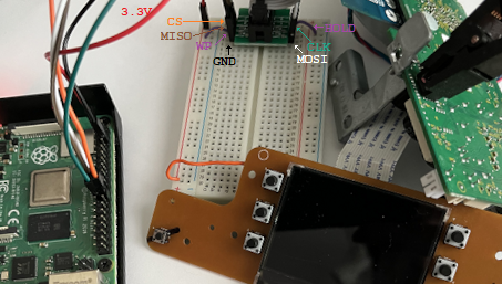
The Linux ecosystem is home to a wide range of open-source software that we can use to perform the read. If for some reason there wasn't, having the ability to program a reader on Linux is extremely valuable which is something you're just not afforded with closed-source programmers. In this read I'll be using flashrom which has incredible support and can be installed through apt. Flashrom uses /dev/spidevX.Y, and you can verify if this is available by checking if the file exists (/dev/spidev0.0). If not you can use device tree compiler, to check if spidev is disabled via dtc -Ifs /proc/device-tree. You should find spidev under spi, verify that the status is set to "okay". If spidev doesn't exist under spi, then you will likely need to either modify a device tree source file overlay - or recompile the device tree blob that get's loaded (this is what happened with my RISC-V RV Dock). If you have a Raspberry Pi, it provides the friendliness mechanism to enable this interface by using raspi-config.
Dumping the ROM with flashrom
To test to see if everything is working and to detect the memory IC, use:
flashrom -p linux_spi:dev=/dev/spidev0.0
If there was a problem, you will get a message saying "No EEPROM/flash device found". Initially with just my test clip attached, the printer wouldn't even boot up. My suspicion is that with HOLD active, startup was being prevented. I then attempted to attach the test clip after boot, however flashrom just reported the error message above. Interestingly if I disabled WP/HOLD before I pressed the power button and then re-enabled it (just adding the pin back into the breadboard), I would get an error code: 0x83C0000A NOS_LOADER_APP.
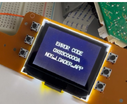
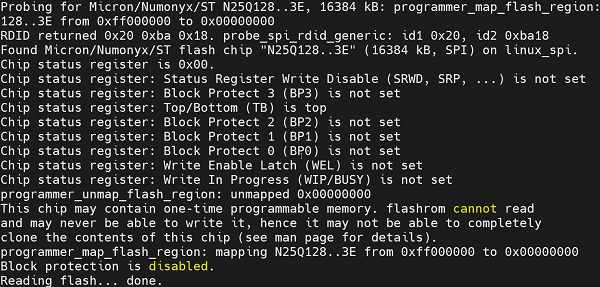
As it turns out, just having power to the board without booting it at all was the solution. On success flashrom had detected that the chip could be a few different models, and then listed them. If this happens then you will need to select the chip which you think it is, and then pass that as the -c argument. Once I selected my chip, I can begin reading which can take a few minutes.
flashrom -p linux_spi:dev=/dev/spidev0.0 -r firmware.bin -VVV
After the succesful read I ran it again but changed the -r argument to -v for verify, which also passed. This firmware dump also matched the hash of my previous extraction using the CH341A from earlier. There are many other different tools and approaches, however I've enjoyed having more flexibility over my CH341A which will now likely just collect dust.
